
Ding! Your 0.1-Nanometer Ultra-Smooth Surface Test Report Has Arrived
Source:
Publish time:
2025-10-21
Ding! Your 0.1-Nanometer Ultra-Smooth Surface Test Report Has Arrived
What Is an Ultra-Smooth Surface?
With the rapid advancement of laser technology and the continuous expansion of laser applications, achieving lower losses in laser systems requires minimizing scattering from optical components within the system. Research has shown that scattering from optical surfaces is proportional to the square of their surface roughness. Therefore, pursuing lower surface roughness is crucial.
Surface roughness refers to the micro-irregularities on a machined surface, characterized by closely spaced peaks and valleys. The distance between two adjacent peaks or valleys (wavelength) is very small (below 1 mm) and cannot be distinguished by the naked eye. This is classified as a microscopic geometric error. The smaller the surface roughness, the smoother the surface becomes[1]. Hence, we commonly refer to the surfaces of optical components with ultra-low surface roughness as "ultra-smooth surfaces". In optical engineering, surfaces with exceptionally low roughness are referred to as ultra-smooth surfaces. Surface roughness is commonly quantified using Ra (arithmetic average deviation of the profile), which represents the arithmetic mean of the absolute values of profile deviations within a specified sampling length—as illustrated in Figure 1.
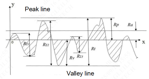
Figure 1. Surface roughness parameters
In the field of precision optical processing, surfaces with a roughness of Ra < 1 nm are typically defined as "ultra-smooth surfaces". To better visualize this standard, consider an analogy: if an optical glass lens were magnified one million times, the requirement would equate to not allowing even a grain of sand-sized pit or protrusion on a 4,000-meter-long airport runway.
The surface roughness levels of optical products vary significantly depending on the processing techniques used. A comparative analysis is provided in Table 1.
Table 1. Surface roughness of products processed by different techniques
Surfaces Processed by different Techniques | Ra | Ra(m) |
Rough-milled surface | 10 μm | 10-5 |
Precision-ground surface | 1 μm | 10-6 |
Conventionally polished surface | 1 nm | 10-9 |
Ultra-smooth surface | 0.1 nm | 10-10 |
Why do we need ultra-smooth surfaces?
In addition to their use in short-wavelength laser systems and as substrates for high-precision ion-beam-sputtered (IBS) coatings, ultra-smooth optical components are now rapidly expanding into two high-growth application areas:
1. With the outlook for autonomous-driving technology becoming clearer, laser gyroscopes for accurately determining a moving vehicle’s orientation are in huge demand. To minimize the influence of light scattering on the gyroscope’s accuracy, all optical parts within the device must possess ultra-smooth surfaces.
2. Laser-induced damage to optical components is a critical issue limiting the development of high-power laser systems, and extensive research has shown that the primary bottleneck affecting the laser damage threshold is the surface roughness of these components. With the growing adoption of ten-kilowatt-class lasers, ultra-smooth surface processing technology capable of achieving 0.1-nanometer-level smoothness has become a highly competitive frontier for major optical component manufacturers.
How are ultra-smooth surfaces measured?
Because the surface roughness of ultra‑smooth surfaces is extremely low, conventional contact scanning with a diamond-tipped stylus no longer meets the required accuracy. High-sensitivity atomic force microscopy (AFM) has sufficient sensitivity but its sampling field is too small, making it suitable for laboratory use rather than industrial production inspection. Therefore, the mainstream method for measuring the roughness of optical components today is white-light interferometry (WLI).
The principle of WLI is to use white-light interference to measure optical path differences, yielding surface error information finer than that obtainable with traditional He–Ne laser interferometers and thus allowing determination of ultra-smooth surface roughness. As shown in Figure 2, the collimated source is split by a beam‑splitting prism into two beams: one is reflected from the test surface and the other from a reference mirror. The reference mirror, driven by a piezoelectric transducer (PZT), is moved vertically in a slow, continuous, and uniform scan to vary the optical path difference between the reference and measurement arms. During the vertical scan, a CCD sequentially captures a series of white‑light interferograms. A 3D topography reconstruction algorithm computes and locates the zero optical path difference position for each pixel to obtain the corresponding height information, thereby reconstructing the specimen’s 3D surface morphology. The analysis software can then read out the required surface roughness Ra value.
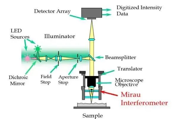
Figure 2. Schematic diagram of white-light interferometry for roughness measurement [2]
CASTECH is equipped with a Zygo NewView 8300 white-light interferometer (Figure 3) based on WLI inspection technology, ensuring stable and reliable measurement of surface-roughness accuracy. Upon customer request, CASTECH can also provide AFM test reports for ultra-smooth-surface products.
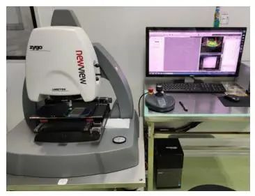
Figure 3. Zygo NewView 8300 white-light interferometer
How are ultra-smooth surfaces manufactured?
Traditional polishing is a process that removes surface layers using abrasive grinding. To achieve higher surface roughness precision, finer abrasives are required. However, research shows that once the surface roughness (Ra) of optical components reaches the 1-nm level, even the finest abrasives cause subsurface damage due to loose polishing debris, hindering further improvement in surface roughness.
Fused-silica optical components are insoluble in water but form an amorphous SiO₂ layer during polishing, known as the Beilby layer. Once formed, this structure protects the surface from subsurface damage caused by abrasive cutting [5].
Leveraging this characteristic, CASTECH has, after years of in-depth research, developed a proprietary process capable of batch-producing ultra-smooth surface components. By strictly controlling the temperature and pH of the polishing liquid, a structurally stable Beilby layer forms on the surface during polishing. Precisely utilizing chemical reactions, the resulting optical components achieve surface roughness (Ra) as low as 0.1 nm. Test results verified by white-light interferometry (WLI) and atomic force microscopy (AFM) are shown in Figures 4 and 5, respectively.
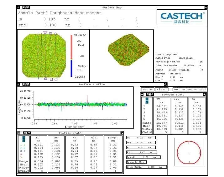
Figure 4. CASTECH Ultra-Smooth Surface Product Measurement Results Using Zygo NewView 8300
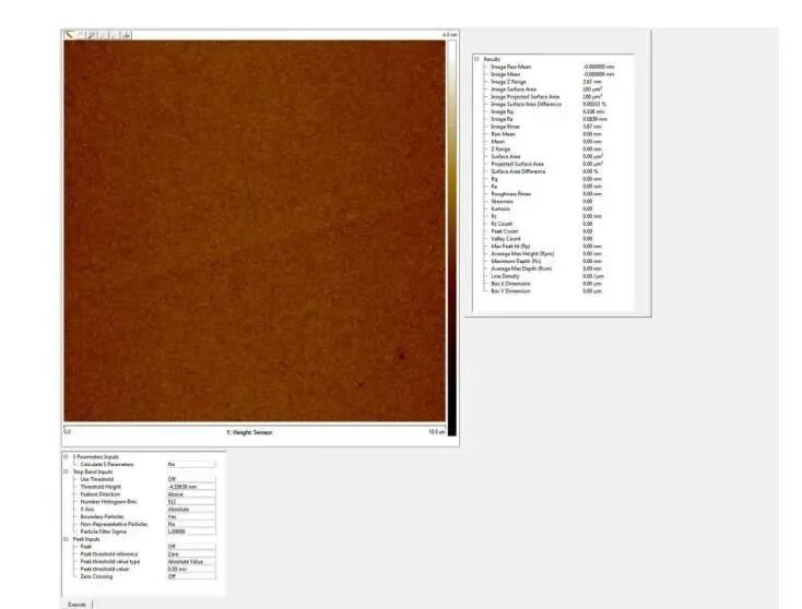
Figure 5. CASTECH Ultra-Smooth Surface Product Measurement Results Using AFM
References:
[1] Cui Wenguang. Design of Surface Roughness Measurement System Based on Laser Speckle [D]. Anhui Xinhua University, 2013.
[2]http://resources.made-in-china.com/article/product-industry- knowledge/MEnQucxPtJlm/Improve-Metrology-for-Sapphire-Substrates-Used-in-LED-Production
[3] Finch, G. Ingle. “The Beilby Layer on Non-Metals.” Nature, vol. 138, no. 3502, 1936, pp. 1010–1010., doi:10.1038/1381010a0.


Related Information